- 您现在的位置:买卖IC网 > Sheet目录2006 > LTC2492IDE#TRPBF (Linear Technology)IC ADC 24BIT DELTA SIG 14-DFN
LTC2492
29
2492fd
APPLICATIONS INFORMATION
In cases where large bypass capacitors are required on
the reference inputs (CREF > 0.01μF) full-scale and linearity
errors are proportional to the value of the reference
resistance. Every ohm of reference resistance produces a
full-scale error of approximately 0.5ppm (while operating
in simultaneous 50Hz/60Hz mode) (see Figures 15 and 16).
If the input common mode voltage is equal to the reference
common mode voltage, a linearity error of approximately
0.67ppm per 100Ω of reference resistance results (see
Figure 17). In applications where the input and reference
RSOURCE (Ω)
0
+FS
ERROR
(ppm) 300
400
500
800
2492 F15
200
100
0
200
400
600
1000
VCC = 5V
VREF = 5V
VIN
+ = 3.75V
VIN
– = 1.25V
fO = GND
TA = 25°C
CREF = 1μF, 10μF
CREF = 0.1μF
CREF = 0.01μF
RSOURCE (Ω)
0
–FS
ERROR
(ppm) –200
–100
0
800
2492 F16
–300
–400
–500
200
400
600
1000
VCC = 5V
VREF = 5V
VIN
+ = 1.25V
VIN
– = 3.75V
fO = GND
TA = 25°C
CREF = 1μF, 10μF
CREF = 0.1μF
CREF = 0.01μF
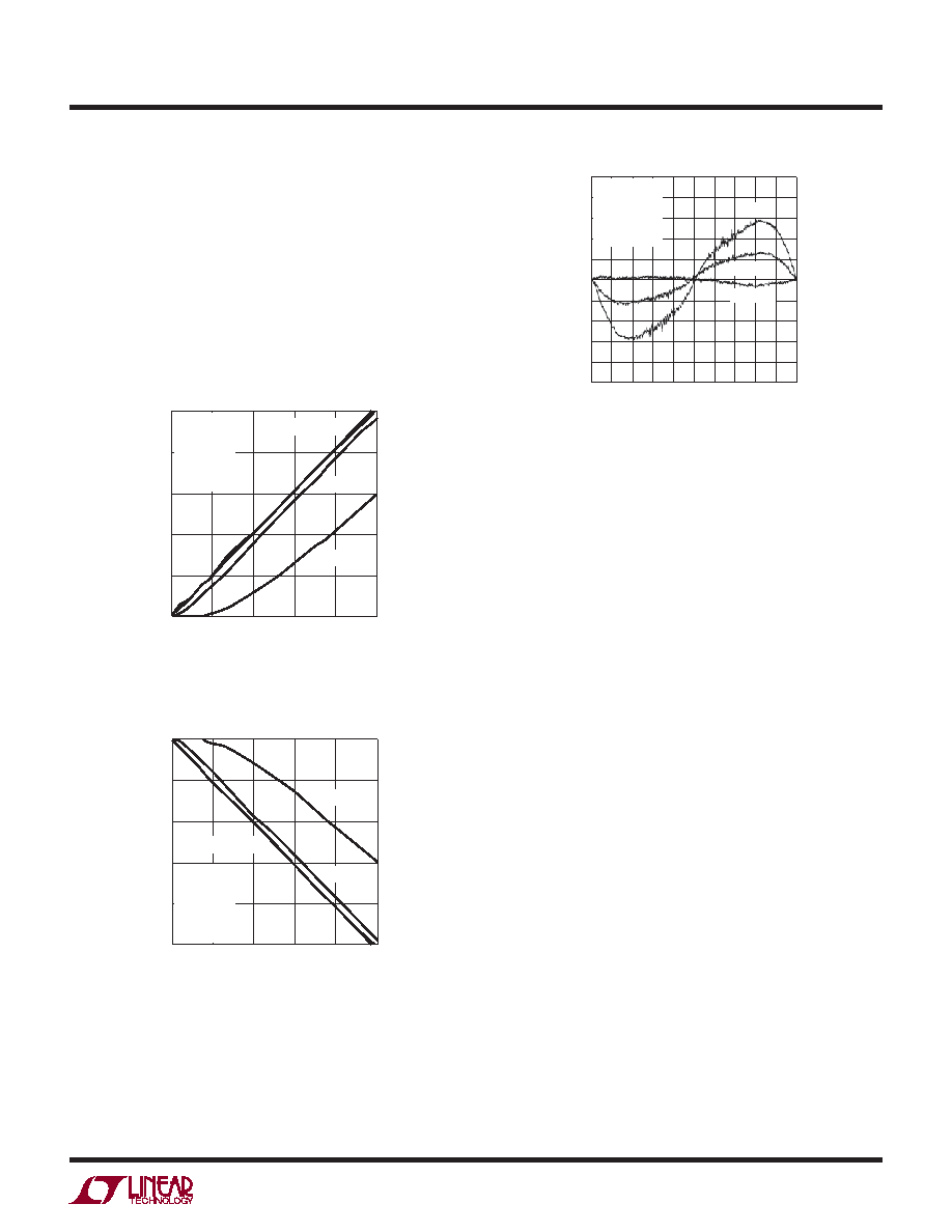
Figure 15. +FS Error vs RSOURCE at VREF (Large CREF)
Figure 16. –FS Error vs RSOURCE at VREF (Large CREF)
VIN/VREF
– 0.5
INL
(ppm
OF
V
REF
)
2
6
10
0.3
2492 F17
–2
–6
0
4
8
–4
–8
–10
– 0.3
– 0.1
0.1
0.5
VCC = 5V
VREF = 5V
VIN(CM) = 2.5V
TA = 25°C
CREF = 10μF
R = 1k
R = 100Ω
R = 500Ω
Figure 17. INL vs Differential Input Voltage and Reference
Source Resistance for CREF > 1μF
common mode voltages are different, the errors increase.
A 1V difference in between common mode input and
common mode reference results in a 6.7ppm INL error
for every 100Ω of reference resistance.
In addition to the reference sampling charge, the reference
ESD protection diodes have a temperature dependent leak-
age current. This leakage current, nominally 1nA (±10nA
max) results in a small gain error. A 100Ω reference
resistance will create a 0.5μV full-scale error.
Normal Mode Rejection and Anti-aliasing
One of the advantages delta-sigma ADCs offer over
conventional ADCs is on-chip digital ltering. Combined
with a large oversample ratio, the LTC2492 signicantly
simplies anti-aliasing lter requirements. Additionally,
the input current cancellation feature allows external low
pass ltering without degrading the DC performance of
the device.
发布紧急采购,3分钟左右您将得到回复。
相关PDF资料
LTC2493IDE#TRPBF
IC ADC 24BIT DELTA SIG 14-DFN
LTC2494IUHF#TRPBF
IC ADC 16BIT W/PGA 38-QFN
LTC2495CUHF#PBF
IC ADC 16BIT W/PGA 38-QFN
LTC2496IUHF#TRPBF
IC ADC 16BIT DELTA SIG 38-QFN
LTC2498IUHF#TRPBF
IC ADC 24BIT 16CH 38-QFN
LTC2600IUFD#PBF
IC DAC OCTAL R-R 16BIT 20-QFN
LTC2602IMS8#TRPBF
IC DAC 16BIT DUAL R-R VOUT 8MSOP
LTC2604IGN-1#TRPBF
IC DAC 16BIT QUAD R-R OUT 16SSOP
相关代理商/技术参数
LTC2493CDE#PBF
功能描述:IC ADC 24BIT DELTA SIG 14-DFN RoHS:是 类别:集成电路 (IC) >> 数据采集 - 模数转换器 系列:- 标准包装:2,500 系列:- 位数:16 采样率(每秒):15 数据接口:MICROWIRE?,串行,SPI? 转换器数目:1 功率耗散(最大):480µW 电压电源:单电源 工作温度:-40°C ~ 85°C 安装类型:表面贴装 封装/外壳:38-WFQFN 裸露焊盘 供应商设备封装:38-QFN(5x7) 包装:带卷 (TR) 输入数目和类型:16 个单端,双极;8 个差分,双极 配用:DC1011A-C-ND - BOARD DELTA SIGMA ADC LTC2494
LTC2493CDE#TRPBF
功能描述:IC ADC 24BIT DELTA SIG 14-DFN RoHS:是 类别:集成电路 (IC) >> 数据采集 - 模数转换器 系列:- 标准包装:2,500 系列:- 位数:16 采样率(每秒):15 数据接口:MICROWIRE?,串行,SPI? 转换器数目:1 功率耗散(最大):480µW 电压电源:单电源 工作温度:-40°C ~ 85°C 安装类型:表面贴装 封装/外壳:38-WFQFN 裸露焊盘 供应商设备封装:38-QFN(5x7) 包装:带卷 (TR) 输入数目和类型:16 个单端,双极;8 个差分,双极 配用:DC1011A-C-ND - BOARD DELTA SIGMA ADC LTC2494
LTC2493CDEPBF
制造商:Linear Technology 功能描述:24bit Delta Sigma ADC Temp Sens LTC2493
LTC2493IDE#PBF
功能描述:IC ADC 24BIT DELTA SIG 14-DFN RoHS:是 类别:集成电路 (IC) >> 数据采集 - 模数转换器 系列:- 标准包装:1 系列:microPOWER™ 位数:8 采样率(每秒):1M 数据接口:串行,SPI? 转换器数目:1 功率耗散(最大):- 电压电源:模拟和数字 工作温度:-40°C ~ 125°C 安装类型:表面贴装 封装/外壳:24-VFQFN 裸露焊盘 供应商设备封装:24-VQFN 裸露焊盘(4x4) 包装:Digi-Reel® 输入数目和类型:8 个单端,单极 产品目录页面:892 (CN2011-ZH PDF) 其它名称:296-25851-6
LTC2493IDE#TRPBF
功能描述:IC ADC 24BIT DELTA SIG 14-DFN RoHS:是 类别:集成电路 (IC) >> 数据采集 - 模数转换器 系列:- 标准包装:1,000 系列:- 位数:16 采样率(每秒):45k 数据接口:串行 转换器数目:2 功率耗散(最大):315mW 电压电源:模拟和数字 工作温度:0°C ~ 70°C 安装类型:表面贴装 封装/外壳:28-SOIC(0.295",7.50mm 宽) 供应商设备封装:28-SOIC W 包装:带卷 (TR) 输入数目和类型:2 个单端,单极
LTC2494CUHF#PBF
功能描述:IC ADC 16BIT W/PGA 38-QFN RoHS:是 类别:集成电路 (IC) >> 数据采集 - 模数转换器 系列:- 标准包装:2,500 系列:- 位数:16 采样率(每秒):15 数据接口:MICROWIRE?,串行,SPI? 转换器数目:1 功率耗散(最大):480µW 电压电源:单电源 工作温度:-40°C ~ 85°C 安装类型:表面贴装 封装/外壳:38-WFQFN 裸露焊盘 供应商设备封装:38-QFN(5x7) 包装:带卷 (TR) 输入数目和类型:16 个单端,双极;8 个差分,双极 配用:DC1011A-C-ND - BOARD DELTA SIGMA ADC LTC2494
LTC2494CUHF#TRPBF
功能描述:IC ADC 16BIT W/PGA 38-QFN RoHS:是 类别:集成电路 (IC) >> 数据采集 - 模数转换器 系列:- 标准包装:2,500 系列:- 位数:16 采样率(每秒):15 数据接口:MICROWIRE?,串行,SPI? 转换器数目:1 功率耗散(最大):480µW 电压电源:单电源 工作温度:-40°C ~ 85°C 安装类型:表面贴装 封装/外壳:38-WFQFN 裸露焊盘 供应商设备封装:38-QFN(5x7) 包装:带卷 (TR) 输入数目和类型:16 个单端,双极;8 个差分,双极 配用:DC1011A-C-ND - BOARD DELTA SIGMA ADC LTC2494
LTC2494IUHF#PBF
功能描述:IC ADC 16BIT W/PGA 38-QFN RoHS:是 类别:集成电路 (IC) >> 数据采集 - 模数转换器 系列:- 标准包装:1 系列:microPOWER™ 位数:8 采样率(每秒):1M 数据接口:串行,SPI? 转换器数目:1 功率耗散(最大):- 电压电源:模拟和数字 工作温度:-40°C ~ 125°C 安装类型:表面贴装 封装/外壳:24-VFQFN 裸露焊盘 供应商设备封装:24-VQFN 裸露焊盘(4x4) 包装:Digi-Reel® 输入数目和类型:8 个单端,单极 产品目录页面:892 (CN2011-ZH PDF) 其它名称:296-25851-6